Optimising your PCB for wireless performance
.
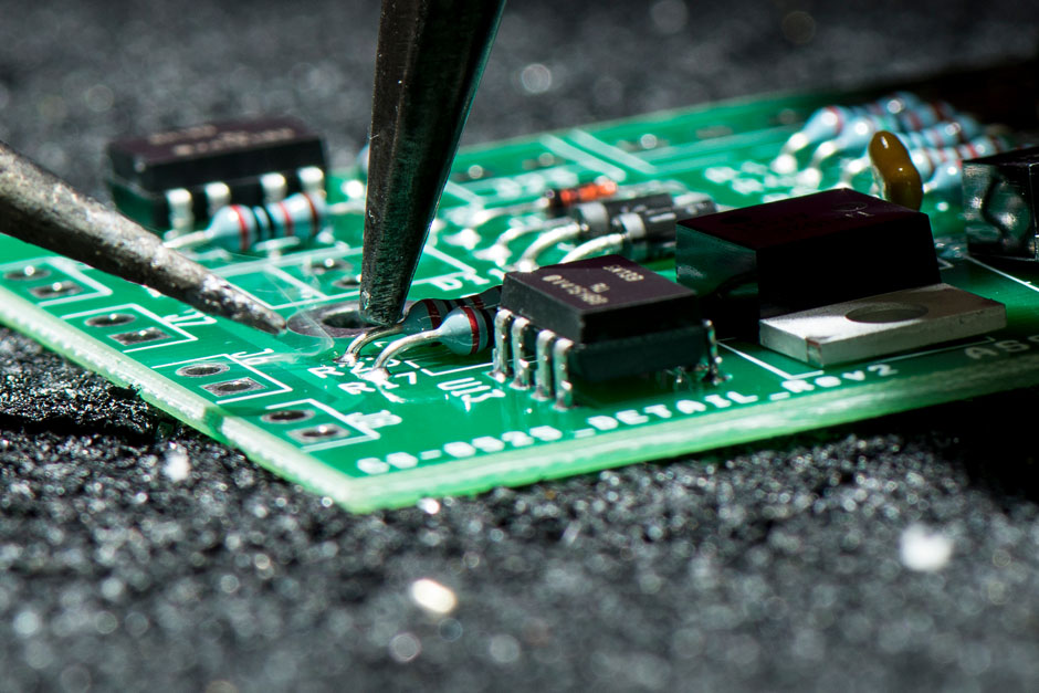
PCB design
Antennas are unlike any other sort of integrated circuit. To achieve strong levels of performance, they require an optimised operating environment. Here are a few factors to consider when starting a printed circuit board design.
Key considerations
Miniaturisation
As devices begin to get smaller and are filled with more components, retaining high levels of performance can be difficult. But there are quick and easy opportunities to optimise a device for wireless performance, particularly if considered from the outset of a project. Embedded antennas offer a great way of minimising PCB real estate while achieving high levels of performance.
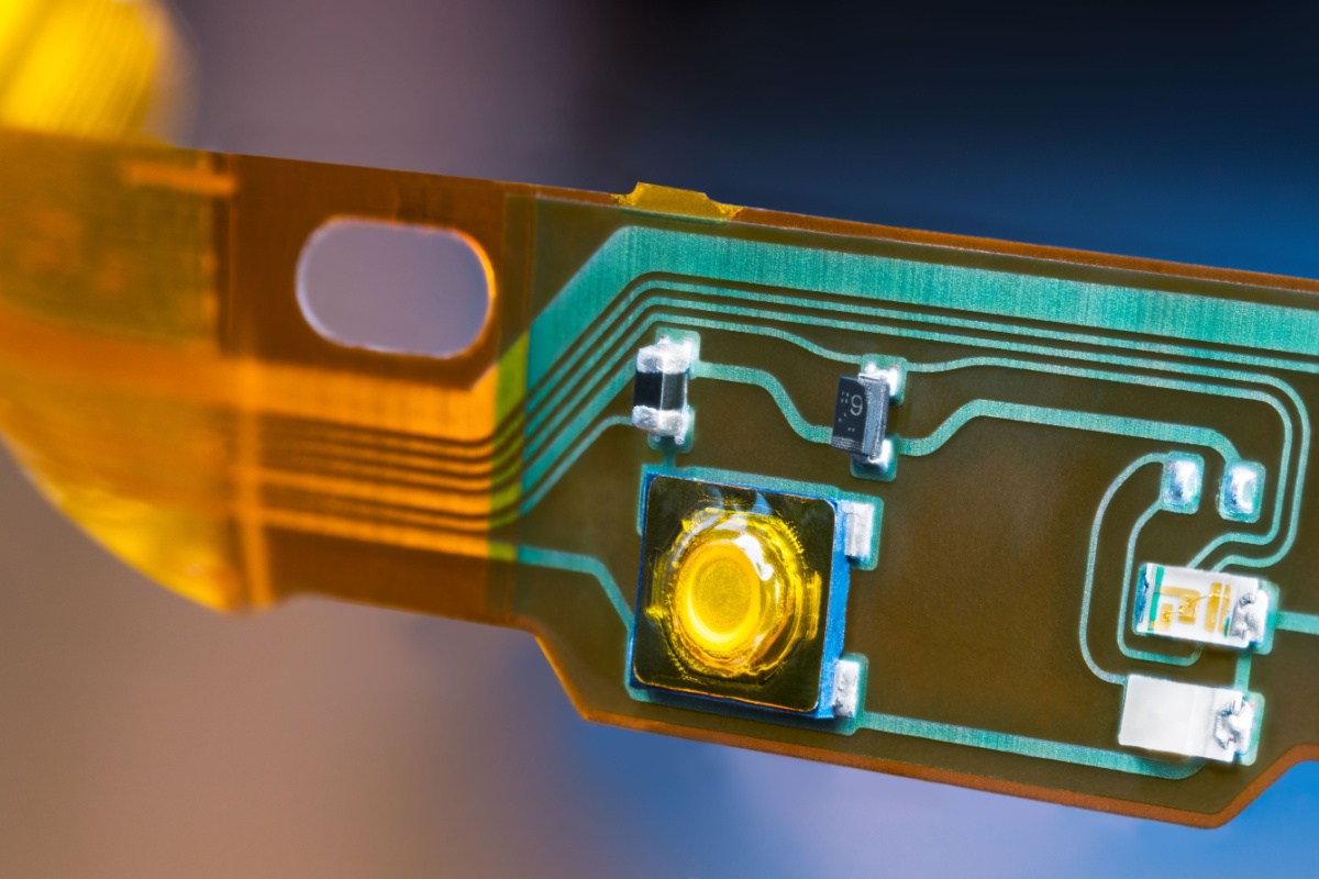
Ground plane space
Component layout
Enclosure material
Enclosure gap
Vias
Transmission line calculator
Get quick, easy and flexible options when selecting the optimum dimensions of your transmission lines.

The ultimate guide to impedence matching
Improperly matched and sub-optimally designed trace lines could substantially reduce wireless performance. Download our whitepaper for more information on impedance matching.

ask.antenova
ask.antenova is a global forum for designers and engineers working with wireless technology. Get answers from those who know best.
